- Products & Capabilities

- Simulation Design & EDA

- About
- Resources
The Essential Guide to PCB Gold Fingers


Gold fingers are essential gold-plated edge connectors on PCBs, known for durability and conductivity, crucial for transmitting digital signals in electronics. They come in Electroplated Hard Gold and ENIG types. Used in motherboards, peripherals, and industrial machinery, they adhere to IPC standards ensuring reliable, high-quality connections in modern electronic devices.
In this highly complex world of new-generation electronics, printed circuit boards (PCBs) have become the foundation. In computerized devices, mobile gadgets, and any kind of industrial machinery used in today's modern world, the transmission of digital signals is very important. Gold fingers are the crux of this connectivity; they are narrow, gold-plated connectors positioned along the edges of PCBs. This all-inclusive guide to PCB gold fingers gives all the details to understand gold fingers, their importance, types, the gold-plating process on them, and their diverse applications.
What are Gold Fingers of Printed Circuit Boards?
Gold fingers are the edge connectors in PCBs that are plated in gold. These are interface points into other boards or components for proper communication and flow of power. These fingers are normally made from hard gold, which is to say gold that has been electroplated, so as to take the pushing and shoving in and out without failure. The normal thickness for gold is from 2 to 50 microns. Which thickness should be used is dependent on what application it is being used for.
We use gold for these connectors as it has the best corrosion resistance and is an excellent electrical conductor. It is relatively hard and durable and is often alloyed with nickel or cobalt for even greater hardness and durability, so the fingers are created to be extremely hardy and to survive for long periods under heavy use.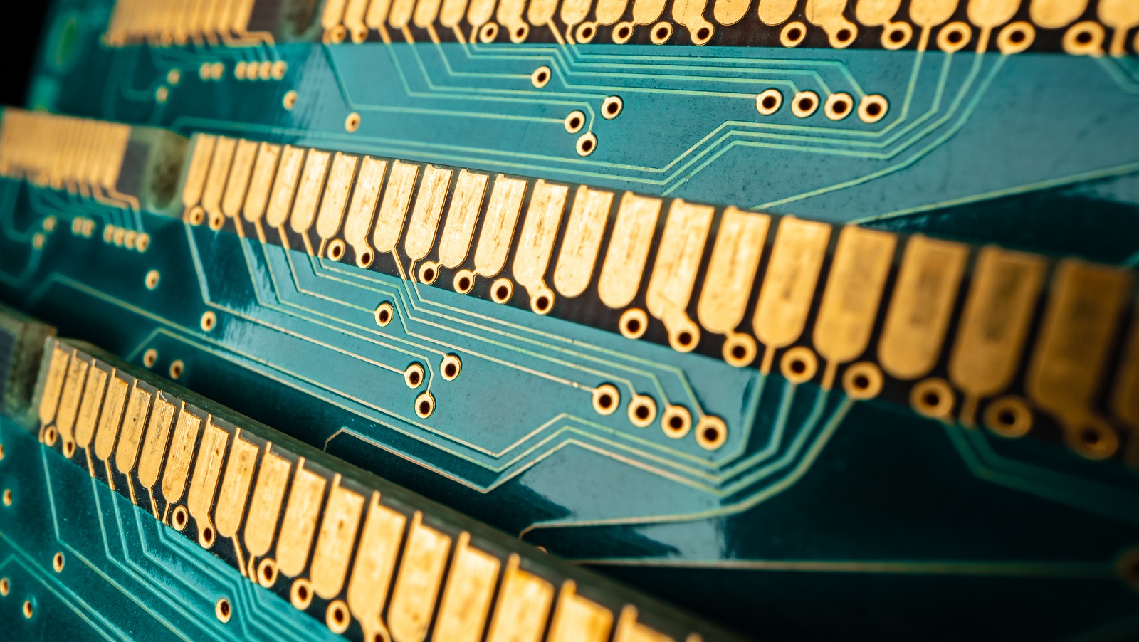
Type of Gold Fingers
The ways of making the finger pads differ mainly in the gold plating thickness and the hardness:
Electroplated Hard Gold: Suited for the most demanding of applications where contacts need to be mated over and over again, this process results in a deposit of approximately 30µ inches of hard gold that has excellent resistance against wear.
Electroless Nickel Immersion Gold (ENIG): Although this process is far more economical than plating with hard gold and easier to solder, the yield golf is much softer and not recommended for most high-abrasion contacts. It's generally plated from 2 to 5µ inches.
The Manufacturing Process: From Concept to Connection
The Gold Fingers Plating process is voluminous and gives a constant high-quality product due to the following important steps: Nickel Plating: This is the first process in which a layer of nickel up to 2 to 6 microns deep is put over the connecting edges of fingers. This base layer acts as a substrate to improve adhesion and endurance of the gold layer, which follows.
Gold Plating: A hard layer of gold (generally compounded with cobalt to make it harder) is electroplated over the nickel. The thickness is in the order 1 to 2 microns.
Beveling: The edges of the fingers are bevelled at a specific angle (usually about 30 to 45 degrees) to enable free entry into their slotted counterparts.
Post-Plating Inspections and Tests
Each PCB undergoes a series of testings and inspection to determine the quality of the gold plating:
Visual Inspection: This is done using magnifying glasses where the smooth and clean contact edges have to be checked.
Adhesion Test (Tape Test): This is done by attaching a strip of the tape to gold plated contact edges, then removing it hence gets inspected for the presence of the gold on the tape hence helps in determining sufficiency in the plating adhesion.
Design and Specifications
Gold finger design on PCBs shall strictly be within specific dimensions and per particular standards for proper performance:
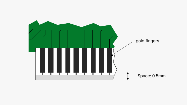
No PTH (plated through-holes) or pads shall be closer than 1mm from the gold fingers
Between the gold fingers and the PCB, there should be a space distance of 0.5mm.
From the edges of the PCB, there shall be at least an exclusion of the inner copper layers so that they don't be exposed during beveling.
The total length for gold fingers for plating has been taken to be of 40mm.
Uses of Gold Fingers
Gold fingers are used in various other sectors. Some of its uses are given below:
In-House Connections: The motherboard is connected to the main PCB with the help of secondary PCB, and such PCB has the gold fingers which slide into the female connections PCI, ISA or AGP.
Special Interfaces: It is used in special booster peripheral equipment such as soundcard and graphics card.
Peripherals: Gold fingers can be found at the edge of the motherboard. The use of gold fingers in the motherboard enables peripheral devices, such as the monitor, printer, USB devices, and even speakers, to be inserted into the motherboard slots, and allows these devices to be frequently plugged and unplugged.
Types of Gold Fingers in Specialised PCBs
Segmented or unequal of gold fingers can exist for special PCBs:
Non-uniform Fingers: For example, in memory card readers, where shorter fingers have been designed so that some parts of the device can receive power supply before other parts.
Segmented Fingers: These segmented connectors are used primarily in rough and waterproof electronics, that too, in very selective applications where a higher degree of rugged utilization is needed.
Gold Finger Standards and Regulations
Association Connecting Electronics Industries–IPC has taken initiatives to develop standards to ensure quality and reliability of PCB gold fingers :
Chemical Composition: The gold plating that is characterized by maximum edge rigidity shall consist of 5 to 10% cobalt.
The gold thickness needs to range from 2 to 50 microinches. Selected single requirements are 0.031 inches, 0.062 inches, 0.093 inches, and 0.125 inches.
Tape and Visual Tests: This will ensure the plating can't be ripped off, plus it's uniform, and adheres well.
The Collision of Technology and Formulation
Currently, gold fingers are used in consumer and industrial machinery, from personal computing devices to manufacturing machinery. Robotic arms and other automated systems get their required power and signal from gold fingers. In consumer electronics, they ensure a smooth interface of so many devices, contributing to techno advancement.
The gold fingers have become the indispensable making element of solid, reliable connections in wide ranges of application inside modern electronics. Due to their excellent conductivity and durability, as well as conformance with high standards, they are applicable in popular devices and complex industrial systems. With great production quality and rigid testing protocols, the manufacturer, Gold Fingers, goes a step further in assisting the big strive for innovations in many fields, which sets the golden standard in PCB technology.
Hot Tags:

Contact us

If you can't find what you're looking for, please contact us.
Article
Through-hole assembly is a key PCB manufacturing technique offering reliability and mechanical strength. This article details design elements, requirements, and standards, including thermal pads, IPC performance levels, component types, solder joint quality, hole sizes, and annular ring dimensions, ensuring robust and manufacturable PCBs for various applications.
 2024/09/11
The article is developed concerning the breakthrough of integrated circuits and the need for custom PCBs in some electronic products. It enumerates ten golden rules in conducting PCB layout design and manufacturing: grid selection, routing, power layers, component placement, panel duplication, component value combination, frequent DRC, flexible silkscreen use, decoupling capacitors, and pre-production parameter checks. These rules provide for the optimum design and manufacturing of a PCB.
2024/07/25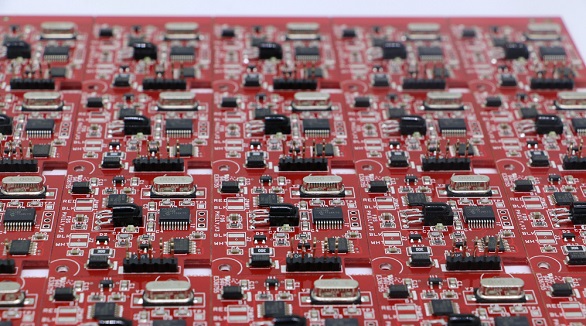
Thermal management is all about more than just keeping the temperature of electronic systems and printed circuit boards low. It has been a key issue related to reliability and performance. Of the very basic fundamentals that would be studied in the field, some are concerned with methods of heat transfer. These are through conduction, convection, and radiation. The methods of cooling include natural cooling, forced-air cooling, fluid cooling, and evaporation cooling. Appropriate thermal design rules shall be followed wherein the chosen materials provide optimum thermal conductivity and the components of a system are so laid out that no hot-spotting will take place. Thermal analysis becomes critical in pointing out heat-related issues and optimizing the design. It thus minimizes failure rates and enhances stability and functionality of the electronic systems through comprehensive thermal management.
2024/07/25